Micro-Electro Mechanical Systems (MEMS) was first used heavily in the sensor industry, its success led to many tiny and well controlled devices.
In the optical domain, MEMS components are widely used for telecommunication industry and optical sensor technology.
There are four main device application areas in the telecom industry.
- Amplifiers
- Switches and optical cross connectors (OXC)
- Filters
- Variable optical attenuators (VOA)
Although many optical MEMS devices are driven by the telecom industry, other research and industry areas have also taken advantage of MEMS devices.
Optical spectroscopy is one of this fields. When high spectroscopic resolution is required, optical spectrometers are still relatively big. The same applies to infrared spectroscopes where almost no small solutions are available.
There are quite a few technologies being used for MEMS fabrication. The major ones are listed below.
- Bulk micromachining
- Surface micromachining
- Hybrid surface/bulk micromachining
- Silicon-on-insulator (SOI)
- LIGA (Lithography, Electroplating, molding)
Bulk Micromachining
Silicon of course has been the star of the IC industry, but it is also a superior substrate for making mechanical structures, thanks to its great mechanical strength (close to steel’s).
So people have used wet chemical etching, dry etching such as reactive ion-beam etching (RIE), laser and focused ion-beam machining as bulk micromachining technique.
Wet chemical etching
In wet chemical etching, the obtained shapes are determined by the chemicals used, the crystal plane of the silicon substrate, and the dopants in the silicon.
The following figure shows the common etching geometries obtained from different crystal planes in the wet chemical etching process.

The silicon substrate is patterned with a masking material that has a much slower etching rate than silicon (using photolithography procedure)
Silicon V-grooves are made this way. V-grooves are commonly used for highly precise fiber or fiber array alignment in fiber optic components.
Using a highly anisotropic etching process, the etching shape of the V-grooves can be precisely controlled by the photo-lithographically patterned masks and etching time.


Reactive Ion-beam Etching (RIE)
In RIE process, photolithographically defined masks are used to pattern the structures, and all unwanted parts are removed by the ion beam.
This technique can create tall structures. The following picture shows a micro-mirrors design for 2x2 optical switches.
The 2x2 OXC has two input and two output fibers. In the MEMS component, the four fibers sit in 75µm high U-grooves and are oriented at right angles to each other.
Their endfaces all meet at one point, where a movable gold-coated mirror is located. This way, the light of either one of the input fibers can be switched to either one of the output fibers.
To enhance the optical performance and minimize the loss, all the optical components are completely surrounded by refractive index matching fluid. The device is placed into a hermetically sealed housing to prevent leaking of the fluid.
The refractive index matching fluid reduces two effects that increase the coupling efficiency between the fibers.
- The index step between the fiber endfaces and the ambient
- The divergence of the freely propagating light in the ambient and hence the beam diameter.
The mirror is attached to a long beam that is electrostatically actuated by comb drives. The optical and mechanical performance of this switch is very good. The insertion loss is between 0.3 and 0.5 dB. The switching time is about 500 µs. The cross talk between the fibers is as low as -70 dB. There is no polarization dependence of the coupling efficiency.

Laser and focused ion-beam(FIB) machining
In this process, high-energy lasers or ion beams are focused into a tiny spot and structures are sculptured out of the substrate.

FIB systems operate in a similar manner to a SEM (scanning electron microscope) except that FIB uses a finely focused beam of ions (usually gallium) that can be operated at high beam currents for site specific sputtering.
Ions are positive, large, heavy and slow, this means that ion beams can remove atoms from the substrate. And because the ion beam position, and size are so well controlled, it can be applied to remove material locally in a highly controlled manner, down to the nanometer scale.
This process doesn’t need masks, however, precise motion control between the beams and the substrate is critical.
Surface Micromachining
Bulk micromachining can achieve high-quality mechanical and optical structures, however, its simplicity also limits its flexibility in achieving versatile structures. And that is when surface micromachining offers complementary advantages.
Surface micromachining uses photolithography to define patterns that are subsequently selectively subjected to chemical processing steps that define the geometries of overlying thin films deposited on the substrate.

In this process, alternating structure and sacrificial (later to be removed) materials are deposited epitaxially and patterned photolithographically on the silicon substrate. Vias and connection holes between structural layers are included in this process.
The wafer is then put into release etching process to selectively remove sacrificial materials. The sacrificial material should have a very high etching rate while the structural material should have a negligible etching rate.
After the whole process, complicated movable structures are created which can be used as sensors or actuators.
The following picture shows a micro-motor which is made by surface micromachining technique.

Most of the surface micromachining structures are limited to two-dimensional planes due to the in-plane geometry of the thin epitaxial layers. However, the surface-micromachined micro-hinges (shown below) allow three-dimensional structures to be created out of in-plane epitaxial growth.

This process consists of two structural polysilicon layers and two sacrificial PSG layers. After the release etching, the POLY2 hinge stapes, the polysilicon plate patterned on the POLY1 layer can be rotated out of the substrate, forming a three-dimensional structure.

This technique has been widely used to make three-dimensional integrated micro-optics, such as micro-mirrors, micro-lenses, and micro-gratings, on a silicon substrate.
Hybrid Bulk/Surface Micromachining
Surface micromachining and bulk micromachining offer complementary advantages. Surface micromachining is flexible and can achieve various actuator and sensor structures, while bulk micromachining can make robust and high-quality mechanical structures.
Traditionally these two processes are difficult to integrate since they use quite different materials and processing principles. However, people have used wafer bonding technique to integrate them and achieved very good result.
This process integrates high quality mechanical structures, such as flat and smooth mirrors made of single crystal silicon, with surface micromachined high-functional actuators and sensors.
The following picture shows the general process.

- Two wafers are first processed separately by surface micromachining and bulk micromachining. An SOI (silicon-on-insulation) wafer with thinned substrate is used in the bulk micromachining process.
- The SOI bulk micromachined wafer is flip-chip bonded to the surface micromachined wafer.
- Then thinned substrate of the SOI wafer is removed by Deep Reactive Ion-beam Etching (DRIE) (the SiO2 layer works as an etching stop).
- The SiO2 layer is removed with HF acid.
- The active single-crystalline silicon wafer on top is patterned photolithographically
- The remaining photoresist is cleaned by oxygen plasma
- The bonding photoresist is hard baked and cured
- The whole wafer is release etched. The etchant removes the sacrificial layers in the surface-micromachined wafer and releases the mechanical structures
Silicon-On-Insulator (SOI) Process
The big advantage of the SOI technology is its simplicity and small number of process steps, because there is usually only one patterning and one depositing step involved.
The most critical step, however, is the deep reactive ion etching (DRIE) that determines the structure itself and surface roughness of the sidewalls of the crucial optical elements of the device.
The following steps are typically in the process.
- The process starts with an SOI wafer which is a composite of a silicon substrate wafer, a buried silicondioxid (BOX) layer, and a device layer
- The wafer is patterned by DRIE utilizing a positive photoresist mask
- The structures are released by wet-etching the BOX underneath the structures that have to move freely during the actuation
- The metallisation improves the surface conductivity and reflectivity. The structures that are not connected via the patterned silicon are electrically isolated from each other by the BOX pedestals
- Integrated alignment structures such as U-grooves are used for the assembly of optical components, e.g. optical fibers

SOI technology combines the advantage of robustness in bulk micromachining with the benefit of versatility in surface micromachining
With these advantages, SOI technology has been widely explored for micro-mirrors in optical scanning and optical switching.
The following picture shows the cross-section of a gimbal mirror made by SOI technology.

LIGA Process
LIGA stands for lithography, electroplating, and molding. This process uses electroplating to create tall and robust mechanical structures with high aspect ratio above the substrate. This is primarily a non-silicon based technology and requires the use of synchrotron generated x-ray radiation.
Here are the general steps involved.
- A thick layer of resist is photolithographically patterned on top of a thin seed layer (such as titanium) which also serves as a sacrificial layer
- The structural material is electroplated into the patterned holes in the resist, followed by planarization.
- After the resist is dissolved, the formed structure can be used as a mold for mass production
- It can also be released and formed into an actuatable structure after etching the sacrificial metal layer

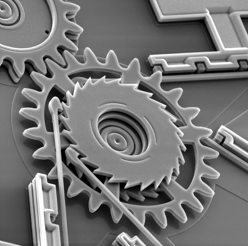
The following picture shows a micro-gear structure, made with LIGA process.

The basic process starts with the cast of an x-ray radiation sensitive PMMA onto a suitable substrate. A special x-ray mask is used for the selective exposure of the PMMA layer using x-rays.
The PMMA is then developed and will be defined with extremely smooth and nearly perfectly vertical sidewalls. Also, the penetration depth of the x-ray radiation into the PMMA layer is quite deep and allows exposure through very thick PMMA layers, up to and exceeding 1 mm.
After the development, the patterned PMMA acts as a polymer mold and is placed into an electroplating bath and Nickel is plated into the open areas of the PMMA. The PMMA is then removed, thereby leaving the metallic microstructure.
Because LIGA requires a special mask and a synchrotron (X-ray) radiation source for the exposure, the cost of this process is relatively expensive.
A variation of the process which reduces the cost of the micromachined parts made with this process is to reuse the fabricated metal part as a tool insert to imprint the shape of the tool into a polymer layer, followed by electroplating of metal into the polymer mold and removal of the polymer mold.
This sequence of steps eliminates the need for a synchrotron radiation source each time a part is made and thereby significantly lowers the cost of the process.