This is a continuation from the previous tutorial - photodetector performance parameters.
Photoemissive detectors are based on the external photoelectric effect. Photoelectrons are emitted when the surface of a metal or a semiconductor, known as a photocathode in this situation, is illuminated with light of a sufficient photon energy.
The lowest vacuum energy level, \(E_\text{vac}\), for an electron freed from the confinement of a material is higher than the Fermi level in the material.
For either a metal or a semiconductor, the energy barrier between the lowest vacuum level and the Fermi level is defined as the work function, \(e\phi=E_\text{vac}-E_\text{F}\), of the material.
For a semiconductor, the difference between the lowest vacuum level and the conduction-band edge is known as the electron affinity, \(e\chi=E_\text{vac}-E_\text{c}\), of the semiconductor.
The quantities \(\phi\) and \(\chi\) have the physical property of an electric potential measured in volts. The work function and the electron affinity of a material are normally measured in electron volts.
Photoemission from a given material occurs only when the incident photon has an energy higher than a certain threshold photon energy, \(E_\text{th}\), corresponding to an optical wavelength shorter than a threshold wavelength, \(\lambda_\text{th}\):
\[\tag{14-53}h\nu\ge{E_\text{th}},\qquad\text{for}\qquad\lambda\le\lambda_\text{th}=\frac{hc}{E_\text{th}}=\frac{1.2398}{E_\text{th}}\text{ μm eV}\]
The values of \(E_\text{th}\) and \(\lambda_\text{th}\) are characteristics of a given material.
- Metal. In a metal, shown in Figure 14-3(a), electrons occupy all of the energy levels below the Fermi level. The threshold photon energy for the emission of a photoelectron from a metal is \[\tag{14-54}E_\text{th}=e\phi\]
- Nondegenerate semiconductor. In a nondegenerate semiconductor, shown in Figure 14-3(b), not all energy levels below the Fermi level, but only those below the valence-band edge, are occupied by electrons because the Fermi level lies within the bandgap. The threshold photon energy for photoemission from a nondegenerate semiconductor is \[\tag{14-55}E_\text{th}=e\chi+E_\text{g}\gt{e\phi},\qquad\text{if }\chi\gt0\]
-
Degenerate semiconductor. In a degenerate semiconductor, the highest level occupied by electrons is the Fermi level. Therefore, the threshold photon energy for photoemission from a degenerate semiconductor is the work function, just like that given in (14-54) for a metal.
For an n-type degenerate semiconductor, \(E_\text{th}=e\phi\lt{e\chi}\), as shown in Figure 14-3(c), because the Fermi level lies in the conduction band.
For a p-type degenerate semiconductor, \(E_\text{th}=e\phi\gt{e\chi+E_\text{g}}\), as shown in Figure 14-3(d), because the Fermi level lies in the valence band.

The work functions of elemental metals are in the range of 2-5 eV. The lowest is that of Cs at 2.1 eV, corresponding to a threshold wavelength of 590 nm for photoemission. Elemental metals have poor quantum efficiencies.
Ordinary group IV and III-V semiconductors, including Si, Ge, GaAs, and InP, have work functions typically in the range of 4-5 eV.
Because of their high threshold photon energies and low quantum efficiencies, elemental metals and ordinary semiconductors are not useful for photocathodes in the visible and infrared spectral regions.
There are two groups of practical photocathodes that have both high quantum efficiencies and low threshold photon energies.
One group consists of compounds of alkaline metals and cesiated silver oxides that are usually labeled with standard international designation of spectral response and window type, such as S-1 (AgOCs), S-4 (Cs3Sb), S-10 (AgBiOCs), S-11 (Cs3Sb), S-20 (Na2KCsSb), and S-24 (Na2KSb).
These compounds are semiconductors that have low threshold photon energies in the range of 1-2 eV because of their small bandgaps and small electron affinities.
Another group consists of negative electron affinity (NEA) photocathodes. An NEA photocathode is made by depositing a very thin n-type layer on the surface of a p-type semiconductor to cause a large downward band bending at the surface.
The photocathode has a negative effective affinity if the band bending is large enough that the conduction-band edge of the p-type semiconductor lies above the vacuum level, as shown in Figure 14-4.
Practical NEA photocathodes have been developed for a few III-V semiconductors by depositing a thin layer of Cs or Cs2O on the surface, including GaAs : Cs2O, InGaAs : Cs, and InAsP : Cs.
As can be seen in Figure 14-4, once an electron is excited to the conduction band of an NEA photocathode, it has sufficient energy to be emitted by tunneling through the thin surface layer.
Therefore, the threshold photon energy for photoemission from an NEA photocathode is simply the bandgap of the semiconductor:
\[\tag{14-56}E_\text{th}=E_\text{g}\]

Figure 14-5 shows the spectral responsivity of typical photocathodes. The spectral responsivity of a photoemissive device has a long-wavelength cutoff determined by the threshold wavelength of the photocathode material and a short-wavelength cutoff determined by the window material.
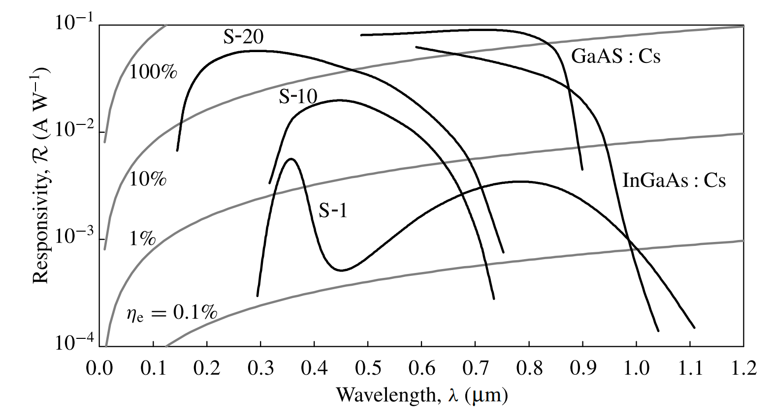
The standard international designation with the letter S, such as S-1, includes both the response of the photocathode material and the transmission of the window material.
Among all practical photocathodes including alkaline compounds and NEA semiconductors, S-1 has the lowest threshold energy of ~1.1 eV, corresponding to a threshold wavelength of ~1.1 μm.
Currently no photocathode can respond at wavelengths longer than 1.2 μm. The spectral response characteristics of the vacuum photodiodes and photomultipliers discussed in the following are completely determined by the spectral response of their photocathodes. Therefore, no photoemissive detectors exist for the infrared at wavelengths longer than 1.2 μm.
Vacuum Photodiodes
The vacuum photodiodes is a simple device that consists of a photocathode and an anode enclosed in a vacuum tube.
The device can use either a reflection-mode photocathode, which is opaque, or a transmission-mode photocathode, which is semitransparent.
The structure of a vacuum photodiode can have either a side-on configuration, with the light incident from the side of the tube, or a head-on configuration, with the light incident from the end of the tube.
The tube can also be filled with a small amount of inert gas, such as argon, to get a small internal gain through ionization of the gas by the collision of photoelectrons. The gas-filled photodiodes are no longer competitive and therefore are not practically useful because they have a limited gain and a low speed.
Figure 14-6(a) shows the basic circuitry of a vacuum photodiode. A voltage, \(V_\text{ak}\), typically a few hundred volts, is applied between the anode and the photocathode to collect the photoelectrons efficiently when the photocathode is irradiated with an optical signal.
Such a high anode voltage is needed to eliminate the space-charge effect between the photocathode and the anode, thus improving the efficiency, and to reduce the electron transit time from the photocathode to the anode, thus increasing the response speed of the device.

The small-signal equivalent circuit, including the noise sources, of a vacuum photodiode is shown in Figure 14-6(b).
A photocathode generates a photocurrent in response to an optical signal. A load resistance, \(R_\text{L}\), is required to convert the photocurrent into an output voltage signal.
The capacitance \(C\) in the equivalent circuit is the total equivalent capacitance from the anode to the ground, including the effects of the anode-to-photocathode capacitance, \(C_\text{ak}\), the anode-to-shield capacitance, \(C_\text{as}\), the photocathode-to-shield capacitance, \(C_{ks}\), and stray capacitance, \(C_\text{p}\), from the output wiring to the ground.
The minimum value of \(C\) is \(C_\text{ak}\), but the other capacitances add to the value of \(C\) and can even become dominant if not carefully minimized.
The dark current of a vacuum photodiode comes from thermionic emission of the photocathode. This dark current is exceedingly small, on the order of femtoamperes at room temperature; it can be ignored in the presence of other noise sources.
The dominant shot-noise sources for a vacuum photodiode are the photocurrent and the background radiation current. The dominant thermal noise is that from the load resistance because the load resistance is much smaller than the internal resistance of a vacuum photodiode.
Ignoring the dark current from thermionic emission, the total noise of a vacuum photodiode is
\[\tag{14-57}\overline{i_\text{n}^2}=2eB(\overline{i_\text{s}}+\overline{i_\text{b}})+\frac{4k_\text{B}TB}{R_\text{L}}\]
where \(i_\text{s}\) is the photocurrent, and \(i_\text{s}=i_\text{ph}\) because a vacuum photodiode has no gain. The NEP of a vacuum photodiode is on the order of 1 fW.
The response speed of a vacuum photodiode is determined by two factors: (1) the transit time and the transit-time spread of the photoelectrons from the photocathode to the anode and (2) the RC time constant of its equivalent circuit shown in Figure 14-6(b).
The transit time is the time for a photoelectron to travel from the photocathode to the anode. The transit-time spread is the spread in the transit time among different photoelectrons caused primarily by the difference in the initial kinetic energies of the photoelectrons when they are emitted from the photocathode.
Both the transit time and the transit-time spread can be reduced by carefully designing the geometry of the device and then by applying a large anode-to-cathode voltage, \(V_\text{ak}\).
For high-speed applications, the RC time constant has to be chosen not to be the limiting factor by using a sufficiently small load resistance, which is typically 50 Ω, and by eliminating all stray capacitances.
The typical speed of a fast vacuum photodiode ranges from 100 ps to 1 ns, with a corresponding 3-dB bandwidth ranging from a few hundred megahertz to about 3 GHz.
Photomultipliers
A photomultiplier tube (PMT) is basically a vacuum photodiode with a built-in high-gain, low-noise electron multiplier.
A PMT consists of four major parts:
- a photocathode for emitting photoelectrons
- an electron optics consisting of focusing electrodes for accelerating and focusing the photoelectrons to the first dynode
- an electron multiplier consisting of a chain of dynodes for secondary electron emission
- an anode to collect the electrons for the output signal.
Depending on the structure of the electron multiplier used in a PMT, there are many different photomultiplier structures, such as the circular cage, the box and grid, the venetian blind, the linear dynode chain, and the microchannel plate, to name a few.
Similarly to a vacuum photodiode, a PMT can use either a reflection-mode or a transmission-mode photocathode and can have either a side-on or a head-on configuration.
Figure 14-7(a) and (b) show, as examples, the configurations and structures of a side-on reflection-mode PMT with a circular-cage structure and a head-on transmission-mode PMT with a box-and-grid structure, respectively.

The electron multiplier of a PMT consists of a series of electrodes, called dynodes, as shown in Figure 14-7(a) and (b). The dynodes are biased at successively higher voltages through a voltage-divider circuit consisting of a series of resistors, as shown in Figure 14-8(a).
When a PMT is used in high-current pulse operation, capacitors are placed in parallel to the resistors in the last two or three stages of the divider circuit. By providing a bypass when the current surges at the peak of the pulse, these capacitors help to maintain constant voltages on the last few dynodes, thus allowing the PMT to have a large linear dynamic range.
Electron multiplication is accomplished by secondary electron emission, which is similar to photoemission except that the incident particle is an electron instead of a photon. Many photocathode materials, including the NEA semiconductors and cesiated oxides, are also used for the dynodes.
A photoelectron emitted from the photocathode is accelerated by the high voltage between the photocathode and the first dynode to an energy of typically 100-200 eV. When such a high-energy electron strikes a dynode, a number of secondary electrons are emitted. This process continues through successive dynode stages.

For a PMT, the total current gain, \(G\), as defined in (14-23) [refer to the photodetector noise tutorial] is the ratio of the output signal current at the anode to the photocurrent at the photocathode.
This gain is given by the total electron multiplication gain through the dynode chain. If the average electron multiplication factor for each dynode stage is \(m\), the total gain for a PMT with a chain of \(n\) dynodes is
\[\tag{14-58}G=\frac{i_\text{s}}{i_\text{ph}}=m^n\]
The total gain can be quite significant even when the single-stage multiplication factor is modest. For example, a ten-stage dynode chain has a gain of \(G\approx10^6\) for \(m=4\) and \(G\approx10^7\) for \(m=5\).
Clearly, a small variation in the multiplication factor \(m\) leads to a large change in the total gain \(G\). Because the value of \(m\) is very sensitive to dynode voltages, both the power supply and the bias circuitry have to be kept very stable for reliable operation of a PMT.
A PMT typically has 9-12 dynode stages biased with a total voltage of 500 V to 3 kV from the anode to the photocathode, depending on the material used for the dynode and the gain desired.
The typical multiplication factor ranges from \(m=3\) to \(8\) for a total gain ranging from \(G=10^3\) to \(10^8\).
Because of the internal gain, the responsivity of a PMT is \(\mathcal{R}=G\mathcal{R}_0\), where \(\mathcal{R}_0\) is the intrinsic responsivity of the photocathode described earlier and shown in Figure 14-5.
The small-signal equivalent circuit, including the noise sources, of a PMT is shown in Figure 14-8(b). Similarly to that in the equivalent circuit of a vacuum photodiode, the capacitance \(C\) is the total equivalent capacitance from the anode to the ground, including the capacitances from the anode to all other electrodes and stray capacitances.
The major source of dark current in a PMT is the thermionic emission from the photocathode and the dynodes. Other less significant sources of dark current include leakage current, field emission, and electron emission by cosmic rays.
The total amplified dark current, \(i_\text{d}\), of a PMT is that at the anode. The anode dark current, \(i_\text{da}\), of a PMT is contributed by the photocathode dark current, \(i_\text{dk}\), amplified by the gain \(G\) and the dark current of all dynodes amplified by a gain less than \(G\).
If we take an effective dynode dark current, \(i_\text{dd}\), such that the the dynode contribution to the anode dark current is equivalently \(Gi_\text{dd}\), the total dark current at the anode can be expressed as
\[\tag{14-59}i_\text{d}=i_\text{da}=G(i_\text{dk}+i_\text{dd})\]
Like that of a vacuum photodiode, the dark current of a PMT is very small. However, the anode dark current of a PMT is detectable and thus cannot be ignored because of the high gain of a PMT.
The total anode dark current \(i_\text{d}\) of a PMT is in the range between 10 pA and 10 nA, depending on the materials of the photocathode and the dynodes and on the operating temperature.
Indeed, the NEP of a PMT is usually limited by the shot noise of its anode dark current. From the discussions in the photodetector noise tutorial, we can then express the shot noise of a PMT as
\[\tag{14-60}\overline{i_\text{n,sh}^2}=2eBG^2F(\overline{i_\text{ph}}+\overline{i_\text{bk}}+\overline{i_\text{dk}}+\overline{i_\text{dd}})=2eBGF(\overline{i_\text{s}}+\overline{i_\text{b}}+\overline{i_\text{d}})\]
where \(i_\text{b}=Gi_\text{bk}\) is the anode current due to background radiation.
The excess noise factor \(F\) for an \(n\)-stage PMT is a function of the multiplication factor \(m\). For \(m\gt2\),
\[\tag{14-61}F=\frac{m^{n+1}-1}{m^n(m-1)}\approx\frac{m}{m-1}\]
Therefore, \(F\) is on the order of unity for a PMT.
Including the thermal noise, the total current noise of a PMT is
\[\tag{14-62}\overline{i_\text{n}^2}=2eBGF(\overline{i_\text{s}}+\overline{i_\text{b}}+\overline{i_\text{d}})+\frac{4k_\text{B}TB}{R_\text{L}}\]
With this total noise, the SNR of a PMT has the form given in (14-33) [refer to the photodetector noise tutorial].
Because of its high gain and low noise, a high-gain PMT can generate an output signal with a good SNR for a single photoelectron emitted by its photocathode. Some PMTs are capable of photon counting and are among the most sensitive photodetectors available.
The NEP of a PMT is typically on the order of 1 fW with a detectivity \(D^*\) on the order of \(10^{16}\text{ cm Hz}^{1/2}\text{ W}^{-1}\). The NEP of a PMT operating in the photon-counting mode can be as low as \(10^{-19}\text{ W}\). A PMT has a large linear dynamic range, typically on the order of 60-80 dB.
The response speed of a PMT is determined by the same two factors that limit the speed of a vacuum photodiode discussed earlier.
Because of the dynode chain, the electron transit time from photocathode to anode in a PMT is much longer than that in a vacuum photodiode and is typically in the range of 10-100 ns.
The transit-time spread, however, is much less than the transit time, typically ranging from 100 ps to about 2 ns.
In terms of the impulse response, the long transit time causes a delay in the response, but the risetime of the response pulse is primarily determined by the combined effect of the transit-time spread and the RC time constant of the PMT circuit.
Therefore, the risetime of a PMT is typically on the order of a few nanoseconds and can be as short as 1 or 2 ns, which is somewhat greater than the transit-time spread but is much less than the electron transit time.
Consequently, a PMT is a very fast detector with a frequency bandwidth on the order of a few hundred megahertz. Combining its high speed with its large gain, a PMT is a superb photodetector that has a gain-bandwidth product unmatched by other types of photodetectors though it is not the fastest photodetector.
Example 14-8
A PMT has a side-on configuration and nine dynode stages. Its photocathode has an effective area of 8 mm x 24 mm and an external quantum efficiency of \(\eta_\text{e}=23\%\) at \(\lambda=400\text{ nm}\).
In a typical operating condition with a voltage of 1 kV applied across the anode and the photocathode, the PMT has the following operating parameters:
The average electron multiplication factor per stage is \(m=6\); the anode dark current is 2 nA; the transit time is 22 ns; the transit-time spread is 1.2 ns; the impulse-response risetime is 2.2 ns; the total equivalent capacitance is \(C=6\text{ pF}\); the background radiation current is negligible.
Answer the following questions for the PMT response at \(\lambda=400\text{ nm}\).
(a) Find the intrinsic responsivity of the photocathode.
(b) What are the gain and the responsivity of the PMT?
(c) Find the NEP for the bandwidth of 1 Hz and the specific detectivity of the PMT by assuming a large load resistance.
(d) What are the cutoff frequency, \(f_\text{3dB}\), and the internal bandwidth, \(B\), of the PMT?
(e) What is the limitation on the load resistance for high-speed applications of the PMT?
(a)
At \(\lambda=400\text{ nm}\), the photon energy
\[h\nu=\frac{1239.8}{400}\text{ eV}=3.1\text{ eV}\]
With \(\eta_\text{e}=23\%\), the intrinsic responsivity of the photocathode at \(\lambda=400\text{ nm}\) is
\[\mathcal{R}_0=\eta_\text{e}\frac{e}{h\nu}=0.23\times\frac{1}{3.1}\text{ A W}^{-1}=74.2\text{ mA W}^{-1}\]
(b)
For \(n=9\) and \(m=6\), the gain
\[G=m^n=6^9=1.0\times10^7\]
Therefore, the responsivity of the PMT at \(\lambda=400\text{ nm}\) is
\[\mathcal{R}=G\mathcal{R}_0=1.0\times10^7\times74.2\text{ mA W}^{-1}=742\text{ kA W}^{-1}\]
(c)
Thermal noise can be ignored for a PMT when the load resistance is sufficiently large. Because the background radiation noise is also negligible, the NEP of the PMT is dark-current limited. For \(m=6\), we find from (14-61) that the excess noise factor is \(F=1.2\). Thus, with \(i_\text{d}=2\text{ nA}\), we have
\[\begin{align}\overline{i_\text{n}^2}&=\overline{i_\text{n,sh}^2}=2eBGF\overline{i_\text{d}}\\&=2\times1.6\times10^{-19}\times1.0\times10^7\times1.2\times2\times10^{-9}\times{B}\text{ A}^2\text{ Hz}^{-1}\\&=7.68\times10^{-21}B\text{ A}^2\text{ Hz}^{-1}\end{align}\]
Then, the NEP for a bandwidth of 1 Hz is
\[\frac{\text{NEP}}{B^{1/2}}=\frac{\overline{i_\text{n}^2}^{1/2}}{B^{1/2}\mathcal{R}}=\frac{(7.68\times10^{-21})^{1/2}}{7.42\times10^5}\text{ W Hz}^{-1/2}=0.118\text{ fW Hz}^{-1/2}\]
The active area of the photocathode is \(\mathcal{A}=8\times24\text{ mm}^2=1.92\times10^{-4}\text{ m}^2\). Therefore, the specific detectivity of the PMT is
\[\begin{align}D^*&=\frac{(\mathcal{A}B)^{1/2}}{\text{NEP}}=\frac{(1.92\times10^{-4})^{1/2}}{0.118\times10^{-15}}\text{ m Hz}^{1/2}\text{ W}^{-1}\\&=1.17\times10^{14}\text{ m Hz}^{1/2}\text{ W}^{-1}\\&=1.17\times10^{16}\text{ cm Hz}^{1/2}\text{ W}^{-1}\end{align}\]
(d)
The cutoff frequency is determined by the risetime, which is \(t_\text{r}=2.2\text{ ns}\). Thus
\[f_\text{3dB}=\frac{0.35}{2.2\times10^{-9}}\text{ Hz}=159\text{ MHz}\]
We then find that
\[B=\frac{f_\text{3dB}}{0.886}=\frac{159}{0.886}\text{ MHz}=180\text{ MHz}\]
Note that the transit-time spread of 1.2 ns contributes to a large part of the risetime of 2.2 ns. The transit time of 22 ns is 10 times the risetime, but it has no consequence on either the risetime or the bandwidth of the PMT.
(e)
For high-speed applications of the PMT, it is required that the circuit RC time constant of the PMT be much smaller than the intrinsic response time of the PMT.
More precisely, the RC-time-limited 3-dB cutoff frequency of the circuit response is required to be much higher than the intrinsic cutoff frequency of the PMT.
As we shall see later, the RC-time-limited 3-dB cutoff frequency
\[f_\text{3dB}^\text{ckt}=\frac{1}{2\pi{R_\text{L}}C}\]
To make sure this PMT is not limited by the RC time, we need \(f_\text{3dB}^\text{ckt}\gg159\text{ MHz}\). With \(C=6\text{ pF}\), we find the following limitation for the load resistance:
\[R_\text{L}\ll\frac{1}{2\pi\times6\times10^{-12}\times159\times10^{6}}\text{ Ω}=167\text{ Ω}\]
Thus a typical choice of \(R_\text{L}=50\text{ Ω}\) will satisfy this requirement for high-speed applications of the PMT.
Even when the load resistance is chosen to be so low, the PMT still operates in the quantum regime with a \(D^*\) limited by the shot noise from its dark current.
If speed is not a concern, a large \(R_\text{L}\) is usually chosen for the PMT to have a large dynamic range.
The next tutorial covers the topic of photoconductive detectors.